We have compiled a list of manufacturers, distributors, product information, reference prices, and rankings for Ion Mass Spectrometer.
ipros is IPROS GMS ・ IPROS One of the largest technical database sites in Japan that collects information on.

Ion Mass Spectrometer Product List and Ranking from 5 Manufacturers, Suppliers and Companies | IPROS GMS

Last Updated: Aggregation Period:Sep 02, 2026~Sep 29, 2026
This ranking is based on the number of page views on our site.

Ion Mass Spectrometer Manufacturer, Suppliers and Company Rankings

Last Updated: Aggregation Period:Sep 02, 2026~Sep 29, 2026
This ranking is based on the number of page views on our site.

  1. 一般財団法人材料科学技術振興財団 MST Tokyo//Testing, Analysis and Measurement
  2. 東芝ナノアナリシス Kanagawa//Testing, Analysis and Measurement
  3. アイテス Shiga//Electronic Components and Semiconductors
  4. 4 イオンテクノセンター Osaka//Testing, Analysis and Measurement
  5. 5 トヤマ Kanagawa//Testing, Analysis and Measurement

Ion Mass Spectrometer Product ranking

Last Updated: Aggregation Period:Sep 02, 2026~Sep 29, 2026
This ranking is based on the number of page views on our site.

  1. [Analysis Case] Imaging of the Cuticle 一般財団法人材料科学技術振興財団 MST
  2. Dynamic SIMS アイテス
  3. [Analysis Case] Depth Profile Analysis of Dopant Elements in SiC Using SIMS 2 一般財団法人材料科学技術振興財団 MST
  4. [Analysis Case] Evaluation of Metal Impurities in the Metal Film and Interface of the Device 一般財団法人材料科学技術振興財団 MST
  5. [Presentation] Surface analysis applicable in various fields! TOF-SIMS Analysis Case Studies 一般財団法人材料科学技術振興財団 MST

Ion Mass Spectrometer Product List

1~16 item / All 16 items

Displayed results

Quantification of Si(1-x)Gex samples with compositional gradient.

Analyze three or more samples with known concentration to solve the problem of two points.

SIMS (Secondary Ion Mass Spectrometry) is used to accurately quantify the concentration distribution of Ge in Si(1-x)Gex films with a compositional gradient used in devices, in the depth direction. When analyzing Si(1-x)Gex films with SIMS, there are two issues that must be resolved. The first issue is that the secondary ion intensity of Ge relative to Si changes significantly with variations in the compositional ratio, so it is necessary to determine the relative sensitivity factor for each compositional ratio. The second issue is that the sputtering rate at each analysis point changes due to variations in the compositional ratio of Si and Ge, so it is necessary to establish the relationship between the compositional ratio and the sputtering rate. To solve these two issues, samples with known concentrations were analyzed at more than three points, and the RSF and sputtering rates were determined. *For more details, please refer to the PDF document or feel free to contact us.*

  • others
  • Ion Mass Spectrometer

Added to bookmarks

Bookmarks list

Bookmark has been removed

Bookmarks list

You can't add any more bookmarks

By registering as a member, you can increase the number of bookmarks you can save and organize them with labels.

Free membership registration

Case Studies on Depth Resolution Measurement in Compound Semiconductor Superlattice Samples

Results of depth resolution measurements using compound semiconductor superlattice samples are published!

This case study collection presents the results of depth resolution measurements conducted by Ion Tech Center Co., Ltd., which provides services such as ion implantation, film formation and analysis, and research and commercialization management. Using Q-pole SIMS (ULVAC: ADEPT-1010), we employed a compound semiconductor sample of Al0.28Ga0.72As/GaAs that was deposited by molecular beam epitaxy (MBE) in 50nm increments to obtain the results of depth resolution. [Overview of Contents] ■ Results of Depth Resolution Measurements *For more details, please refer to the catalog or feel free to contact us.*

  • others
  • Contract measurement
  • Other contract services
  • Ion Mass Spectrometer

Added to bookmarks

Bookmarks list

Bookmark has been removed

Bookmarks list

You can't add any more bookmarks

By registering as a member, you can increase the number of bookmarks you can save and organize them with labels.

Free membership registration

FIB Light Ionization Nano Mass Imaging Device "FILMER"

Equipment using laser SNMS that achieves optical spatial resolution for environmental particle analysis and more!

Toyama's "FILMER" is a flight time secondary ion mass spectrometer that meets the needs of research and development in the field of polymer materials and organic-inorganic composite materials. It achieves a high spatial resolution with a mapping surface resolution of 50 nm, while also maintaining a mass resolution (m/Δm): 5,000 @ m/z = 56. By adopting laser SNMS, it improves the signal ion generation efficiency, enabling highly sensitive analysis of organic materials. [Features] ■ Achieves high spatial resolution ■ Capable of in-situ processing and analysis ■ Adopts laser SNMS *For more details, please refer to the PDF document or feel free to contact us.

  • Analytical Equipment and Devices
  • Environmental Test Equipment
  • Other physicochemical equipment
  • Ion Mass Spectrometer

Added to bookmarks

Bookmarks list

Bookmark has been removed

Bookmarks list

You can't add any more bookmarks

By registering as a member, you can increase the number of bookmarks you can save and organize them with labels.

Free membership registration

[Analysis Case] Evaluation of Element Distribution in Oxide ReRAM Operating Area Using SIMS

High-sensitivity evaluation of local elemental distribution in oxide devices using oxygen isotopes.

In oxide ReRAM, it was suggested that oxygen diffusion associated with the application of an electric field is related to memory operation (resistance change). Since SIMS analysis allows for the measurement of isotopes, utilizing the isotope 18O ion implantation technique enables the tracking of oxygen diffusion. For devices where 18O was locally implanted, a bridge structure that serves as the operating region was formed by applying an electric field, and elemental mapping revealed that the intensity of 18O in the bridge area was weak, indicating localized reduction.

  • Contract Analysis
  • Ion Mass Spectrometer

Added to bookmarks

Bookmarks list

Bookmark has been removed

Bookmarks list

You can't add any more bookmarks

By registering as a member, you can increase the number of bookmarks you can save and organize them with labels.

Free membership registration

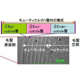
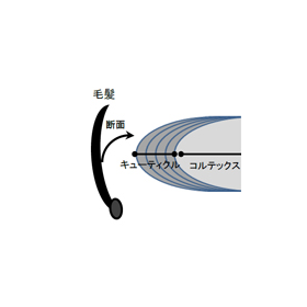
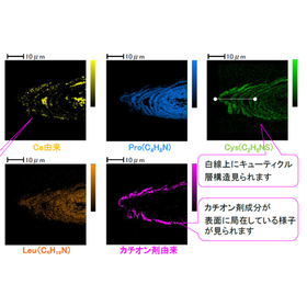
[Analysis Case] Imaging of the Cuticle

It is possible to evaluate the distribution of components in the hair cuticle!

Our organization offers imaging of cuticles. The evaluation of cuticles has been limited to structural observation using electron microscopy due to their fine structure, and detailed component distribution has remained unclear. By using TOF-SIMS, which can evaluate the distribution of inorganic and organic materials at the sub-micron level, it is possible to assess the distribution of various components within the cuticle. This document presents the results of evaluating hair and visualizing the component distribution within the cuticle. [Measurement and Processing Method] ■ [TOF-SIMS] Time-of-Flight Secondary Ion Mass Spectrometry *For more details, please download the PDF or feel free to contact us.

  • 5a.png
  • 5b.png
  • 5c.png
  • Contract Analysis
  • Ion Mass Spectrometer

Added to bookmarks

Bookmarks list

Bookmark has been removed

Bookmarks list

You can't add any more bookmarks

By registering as a member, you can increase the number of bookmarks you can save and organize them with labels.

Free membership registration

[Presentation] Surface analysis applicable in various fields! TOF-SIMS Analysis Case Studies

From inorganic to organic materials, leave high-sensitivity surface analysis to us!

TOF-SIMS analysis allows for detailed examination of the sample's outermost surface, as well as the ability to obtain information in the depth direction, making it possible to understand the distribution of components within the material. Additionally, imaging can visualize the spatial distribution of components. This document includes case studies of products analyzed from various fields. Please feel free to contact us!

  • Contract measurement
  • Contract Inspection
  • Ion Mass Spectrometer

Added to bookmarks

Bookmarks list

Bookmark has been removed

Bookmarks list

You can't add any more bookmarks

By registering as a member, you can increase the number of bookmarks you can save and organize them with labels.

Free membership registration

[Analysis Case] Diamond Evaluation Case Using SIMS

It is possible to quantitatively evaluate impurity elements and assess film thickness.

Diamonds possess excellent physical properties such as high breakdown electric fields, making them promising materials for next-generation power devices and quantum devices. By doping diamonds with impurity elements, they can function as high-performance semiconductors. To understand the concentration distribution of the doped elements, SIMS analysis, which can detect impurities in the ppb to ppm range with high sensitivity, is effective. Additionally, it is possible to evaluate the film thickness of each layer from the impurity concentration distribution. MST offers a variety of diamond standard samples and can quantify over 30 different elements.

  • img_C0733_1.jpg
  • Contract measurement
  • Contract Inspection
  • Mass Spectrometer
  • Ion Mass Spectrometer

Added to bookmarks

Bookmarks list

Bookmark has been removed

Bookmarks list

You can't add any more bookmarks

By registering as a member, you can increase the number of bookmarks you can save and organize them with labels.

Free membership registration

High-performance automated SIMS

It is possible to provide rapid feedback for process development and defect analysis of semiconductor devices!

Secondary Ion Mass Spectrometry (SIMS) enables depth profiling analysis with high sensitivity and high mass resolution for all elements. Furthermore, our company has added automation features from sample introduction to analysis, allowing for high-precision automated measurements. As a result, we can provide rapid feedback for process development and defect analysis in semiconductor devices, where quick responses are required. 【Features】 ■ High sensitivity measurement: Capable of high sensitivity measurement of heavy elements such as Ag, In, and Sb. ■ High mass resolution measurement ・M/ΔM = ~10,000 ・Evaluation of contamination levels of P, Al, Fe, Ni, etc., in Si and SiO2. *For more details, please download the PDF or feel free to contact us.

  • Other analysis and evaluation services
  • Ion Mass Spectrometer

Added to bookmarks

Bookmarks list

Bookmark has been removed

Bookmarks list

You can't add any more bookmarks

By registering as a member, you can increase the number of bookmarks you can save and organize them with labels.

Free membership registration

Secondary Ion Mass Spectrometry (SIMS)

There are various types of mass spectrometers, such as magnetic field type, quadrupole type, and time-of-flight type, which are used according to the purpose of the analysis!

Secondary Ion Mass Spectrometry (SIMS) is a highly sensitive analytical technique capable of identifying and quantifying trace impurity elements at the ppb level. Since measurements are conducted while sputtering, it is possible to obtain the depth distribution of impurities within the film. Please feel free to contact us when you need assistance. 【Features】 ■ Magnetic Field SIMS: Used for evaluating impurities that require high sensitivity. ■ Quadrupole SIMS: Used for evaluations that require depth resolution and for assessing multilayer films that include insulating films. ■ Time-of-Flight SIMS: Used for evaluating the molecular structure level of trace substances on the surface, as well as for assessing the contamination state of organic materials and minute foreign substances on the surface. *For more details, please download the PDF or feel free to contact us.

  • Other analysis and evaluation services
  • Ion Mass Spectrometer

Added to bookmarks

Bookmarks list

Bookmark has been removed

Bookmarks list

You can't add any more bookmarks

By registering as a member, you can increase the number of bookmarks you can save and organize them with labels.

Free membership registration

High-performance magnetic field SIMS

SIMS equipped with three features: high sensitivity, high mass resolution, and high depth resolution!

The "high-performance magnetic field SIMS" is a device that can analyze all elements with high sensitivity in depth direction. With high-performance SIMS capable of high-sensitivity and high mass resolution analysis even in low-energy analysis, it has become possible to achieve high-precision measurements in challenging, extremely shallow regions. As a result, it can now be applied to semiconductor devices, which are advancing in miniaturization and diversification of materials. 【Features】 ■ High sensitivity measurement (high transmission rate) ■ High mass resolution ■ Various measurements possible from ultra-low energy analysis to standard analysis ■ Equipped with a high-brightness ion gun ■ Automatic measurement with high repeatability precision, capable of measuring up to 25 samples *For more details, please download the PDF or feel free to contact us.

  • Analytical Equipment and Devices
  • Ion Mass Spectrometer

Added to bookmarks

Bookmarks list

Bookmark has been removed

Bookmarks list

You can't add any more bookmarks

By registering as a member, you can increase the number of bookmarks you can save and organize them with labels.

Free membership registration

Dynamic SIMS

Suitable for analysis of glass, metal, ceramics, silicon, compound semiconductors, shallow implants, and more!

"DYNAMIC SIMS" is a secondary ion mass spectrometry method that can detect trace amounts of all elements (from H to U) in samples with high sensitivity, ranging from ppm to ppb. It allows for qualitative analysis and depth profiling, and additionally enables high-precision quantitative analysis using standard samples (conducted at our partner company's facility). The minimum beam diameter is approximately 30 µm, and it can be further reduced depending on the material. 【Features】 ■ Automatic loading/unloading of samples, high throughput (24 samples/load) ■ Unmatched depth profiling capability and high depth resolution, wide dynamic range ■ Optimized for the analysis of glass, metals, ceramics, silicon, compound semiconductors, shallow implants, etc. ■ Highest detection limit: from ppm to ppb (10^-6 to 10^-9) *For more details, please refer to the PDF document or feel free to contact us.

  • ?Depth.png
  • Analytical Equipment and Devices
  • Ion Mass Spectrometer

Added to bookmarks

Bookmarks list

Bookmark has been removed

Bookmarks list

You can't add any more bookmarks

By registering as a member, you can increase the number of bookmarks you can save and organize them with labels.

Free membership registration

[Analysis Case] Depth Profile Analysis of Dopant Elements in SiC Using SIMS 2

Measurements will be taken according to the analysis conditions suited to the purpose.

This paper presents examples of evaluating the depth concentration distribution of the dopant elements N, Al, and P in commercially available SiC power MOSFETs using multiple analysis modes. Depending on the analysis objectives, it is possible to measure multiple elements simultaneously without measuring each element separately under optimal conditions. Examples are provided for cases of simultaneous multi-element measurement and measurements focused on each individual element.

  • Contract Analysis
  • Ion Mass Spectrometer

Added to bookmarks

Bookmarks list

Bookmark has been removed

Bookmarks list

You can't add any more bookmarks

By registering as a member, you can increase the number of bookmarks you can save and organize them with labels.

Free membership registration

[Analysis Case] Depth Direction Analysis of Components in SiON Ultra-Thin Films

It is possible to capture molecular information of inorganic substances in the depth direction using TOF-SIMS.

The SiON film used as the gate oxide film for Si transistors is formed by introducing nitrogen into the Si oxide film to suppress leakage current. To ensure a good interface characteristic with the substrate while maintaining the dielectric constant, it is necessary to strictly control the distribution of nitrogen in the SiON film. We will present a case study evaluating the distribution of silicon oxide and nitride in a 1nm thick SiON film using TOF-SIMS. TOF-SIMS has high depth resolution on the surface and can obtain molecular information with good sensitivity, allowing for a clear understanding of the compositional distribution in the ultra-thin SiON film.

  • img_C0264_2.jpg
  • img_C0264_3_HO-Si-O.jpg
  • img_C0264_4_O-Si-O-Si-O.jpg
  • img_C0264_5_Si-N-Si.jpg
  • img_C0264_6_Si-Si.jpg
  • Contract measurement
  • Transistor
  • Memory
  • Ion Mass Spectrometer

Added to bookmarks

Bookmarks list

Bookmark has been removed

Bookmarks list

You can't add any more bookmarks

By registering as a member, you can increase the number of bookmarks you can save and organize them with labels.

Free membership registration

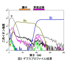
[Analysis Case] Evaluation of Metal Impurities in the Metal Film and Interface of the Device

Impurities in films and interfaces such as plating can be evaluated using TOF-SIMS.

Impurities from components of the film formation device, target materials, and plating solutions can contaminate the device and have adverse effects, making the qualitative assessment of impurities on surfaces, within films, and at interfaces important. TOF-SIMS can sensitively evaluate unknown elements present on surfaces, within films, and at interfaces in a single measurement due to the following three characteristics: 1. For metallic elements, ions from m/z 1 to 800 can be detected simultaneously in one measurement. 2. Detection sensitivity of a few ppm can be achieved (varies depending on materials and ions). 3. The use of a sputter gun allows for the evaluation of depth distribution.

  • img_c0638_2.jpg
  • Wafer
  • Contract measurement
  • Other semiconductors
  • Ion Mass Spectrometer

Added to bookmarks

Bookmarks list

Bookmark has been removed

Bookmarks list

You can't add any more bookmarks

By registering as a member, you can increase the number of bookmarks you can save and organize them with labels.

Free membership registration

Impurity analysis of GaN gate oxide film

Successfully captured impurity diffusion from the upper side of the gate oxide film using D-SIMS!

In GaN devices, the diffusion of components (impurities) originating from the pre-process of the gate oxide film leads to insulation failures, making it necessary to identify their concentration distribution and diffusion sources. We have developed a technology that provides high flatness to the surface of thin-film processed GaN compounds. As a result, we successfully captured the diffusion of impurities from the upper side of the gate oxide film using D-SIMS. *For detailed information, please refer to the attached PDF document. For further inquiries, feel free to contact us.

  • Other analysis and evaluation services
  • Ion Mass Spectrometer

Added to bookmarks

Bookmarks list

Bookmark has been removed

Bookmarks list

You can't add any more bookmarks

By registering as a member, you can increase the number of bookmarks you can save and organize them with labels.

Free membership registration

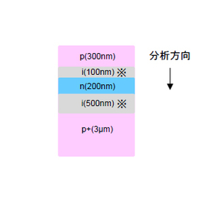
Nitrogen concentration analysis of SiC n-buffer layer

Successfully captured the n-buffer layer thickness and nitrogen (N) concentration using D-SIMS!

In recent years, in SiC MOSFETs, an n-buffer layer on the order of several hundred nanometers has been inserted between the n-substrate and the n-drift layer to address on-resistance issues. In the evaluation of the n-buffer layer, it is necessary to thin the n-drift layer, which is positioned above and is on the order of several micrometers, to improve depth direction resolution and to flatten its surface. We have developed a technology that provides high flatness to the surface of SiC compounds processed as thin films. As a result, we successfully captured the thickness and nitrogen (N) concentration of the n-buffer layer using D-SIMS. *For detailed information, please refer to the attached PDF document. For further inquiries, please feel free to contact us.

  • Other analysis and evaluation services
  • Ion Mass Spectrometer

Added to bookmarks

Bookmarks list

Bookmark has been removed

Bookmarks list

You can't add any more bookmarks

By registering as a member, you can increase the number of bookmarks you can save and organize them with labels.

Free membership registration